Printed Circuit Board Introduction
PCB ( printed circuit board ) is a key component in the electronics industry and it is also a basic component. PCB carries all the components to be PCBA and then becomes the core of every electronic products. This article will give you a general idea about PCB, show the PCB composition and some main aspects.
What is PCB?
PCB(Printed circuit board)is a widely used name.It also can be called as printed wiring boards or printed wiring cards.
Winding technology is a major advancement in circuit technology.It improves the durability and replaceability of the circuit by winding small-diameter wires on the poles of the connected point.
When the electronics industry develops from vacuum tubes and relays to silicon semiconductors and integrated circuits, the size of electronic components is smaller and price are also cheaper. There are more and more lectronic products appeared in consumer field, which prompted the manufacturers to find smaller and more cost-effective solutions. Then, the PCB was born.
Composition
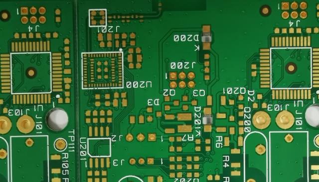
PCB looks like a multi-layer cake or lasagna-layers of different materials are pressed together by heat and adhesives.Let's start from the middle layer.
FR4
The substrate of PCB is generally glass fiber. In most cases, the glass fiber substrate of PCB generally refers to the material FR4. The solid material FR4 makes PCB with hardness and thickness. In addition to the FR4 substrate, there are flexible circuit boards which is produced with flexible high-temperature plastics (polyimide or similar) and so on.
Inexpensive PCBs and hole boards are made of materials such as epoxy resin or phenol, which lack the durability of FR4, but are much cheaper. When soldering things on this kind of board, you will smell a lot of peculiar smell. This type of substrate is often used in very low-end consumer products. Phenolic substances have a low thermal decomposition temperature, and too long welding time will cause them to decompose and carbonize, and emit an unpleasant smell.
High Precision PCB mainly is manufactured with FR4 from KB and Shengyi.The quality is guaranteed.It is widely used for electronic consumer products, telecommunication, industrial control, automotive, LED products and power supply, etc.
Copper
The next introduction is the thin layer of copper foil, which is pressed onto the substrate through heat and adhesive during production. On the double-sided board, the copper foil will be pressed on the front and back sides of the substrate. For some low-cost application, copper foil may only be pressed on only one side of the substrate. When we mention to double-sided board or two-layer board, it means FR4 with two layers of copper foil on the substrate. But for different PCB designs, the number of copper foil layers may be only 1 layer, or even more than 16 layers.
There are many types of copper thickness, and it is calculated by weight. Generally, the weight ( oz ) is calculated by the copper evenly covers one square foot. The copper thickness of widely used PCB is 1oz, but 2oz or 3oz copper thickness are used by some high-power PCBs.1 ounces ( oz ) is about 35um or 1.4mil copper thickness.
High Precision PCB capacibility of base copper thickness is 1/3 oz to 3 oz for outer layer. For inner layer, it can be 1/3 oz to 3 oz.
Soldermask
Above the copper layer is the solder mask. This layer makes the PCB look green. The solder mask layer covers the traces of copper layer to prevent the traces on the PCB from contacting other metals, solder or other conductive objects and causing short circuits. The existence of the solder mask allows solder on the right place and prevents solder bridging.
Generally speaking, solder mask is green, but almost all colors can be used for solder mask.
High Precision PCB can do solder mask which are mainly from Rongda & Taiyo.The color can be green, white, black, yellow, blue, purple, red etc.
Silkscreen
On the top of the solder mask, it is silk screen layer. Letters, numbers and symbols all can be printed on solder mask layer of the PCB to facilitate assembly and guide to understand better the design of the board. It often use symbols on the silk screen layer to mark certain pins or LED functions,and so on.
The most common color of silk screen is white. But the silk screen layer can also be made with almost any color, like black, gray, red or even yellow. However, it is rare to print with multiple silk screen colors on one same board.
High Precision specialise on PCB manufacturing for more than 10 years.Welcome to send us enquiry to consult info@gjzpcb.com
Sales Office: No.912-913 Chengtouxin Time Building,Pingshan Road,Pingshan District,Shenzhen,China
Factory I Add: 1# Southwest Fifth Street,Shijie Town, Dongguan,China
Factory II Add: Industrial Park,Guiyang,Chenzhou City,Hunan,China