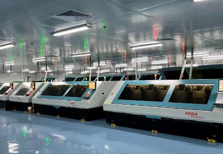
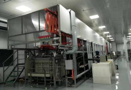
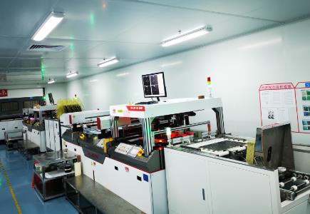
Rigid PCB Manufacturing Process Flow
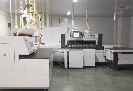
1. Cutting
Cutting is the process of cutting the copper clad laminate into pieces that can be reprocessed in the production process line.
(1) Unit: Unit refers to a single small board designed by PCB design engineers.
(2) Set: Set refers to the unity formed by putting together multiple Units for reasons such as improving production efficiency and facilitating production. This is also the jigsaw we often say, it includes a single small board, process edges and so on.
(3) Panel: Panel refers to a large board formed by putting together multiple sets and adding tool board edges during the production of PCB manufacturers in order to improve efficiency and facilitate production.
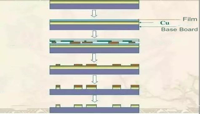
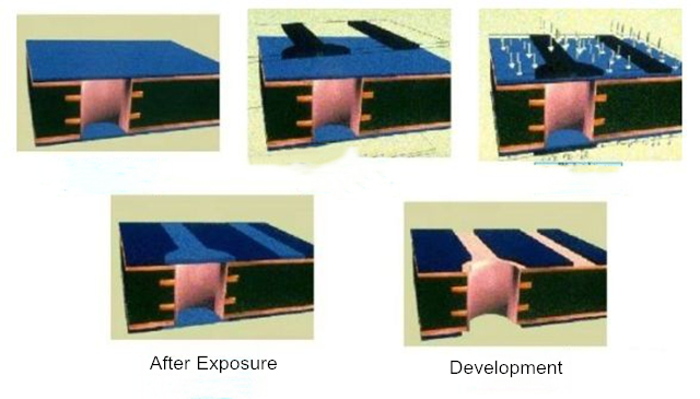
2. Inner Layer Image Transfer
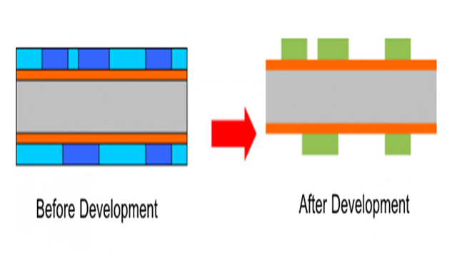
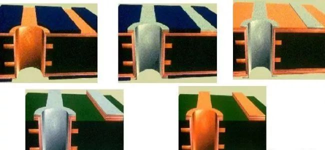
The inner layer image transfer is the process of transferring the inner layer circuit pattern to the PCB board, including multiple processes such as inner layer filming, exposure and development, and inner layer etching. The inner film is to paste a special photosensitive film on the surface of the copper plate, which is what we call a dry film. This film will solidify when exposed to light, forming a protective film on the board. Exposure and development is to expose the board with the film, the light-transmitting part is cured, and the non-light-transmitting part is still the dry film.Then, after developing, the uncured dry film is removed, and the board with the cured protective film is etched. After removing the film, the inner circuit pattern is transferred to the board. The whole process flow is as shown in the figure below.
For designers, our main consideration is the minimum line width of the wiring, the control of the spacing and the uniformity of the wiring. Because the distance is too small, it will cause the film to be sandwiched, and the film cannot be completely removed and cause a short circuit. If the line width is too small, the adhesion of the film is insufficient, resulting in an open circuit. Therefore, the safety distance (including line and line, line and pad, pad and pad, line and copper surface, etc.) of the circuit design must consider the feasibility of production.
A. Pretreatment:
Main function: Solve the problems of surface cleanliness and surface roughness. Remove oxidation, increase the roughness of the copper surface, and facilitate the film to adhere to the copper surface.
B. Laminating.
The processed substrate is pasted with a dry film or a wet film by hot pressing or coating.
C. Exposure.
Align the film with the substrate on which the dry film is pressed, and use the ultraviolet light on the exposure machine to transfer the film pattern to the photosensitive dry film.
D. Development.
Use the weak alkalinity of the developer (sodium carbonate) to dissolve and rinse the unexposed dry film or wet film, leaving the exposed part.
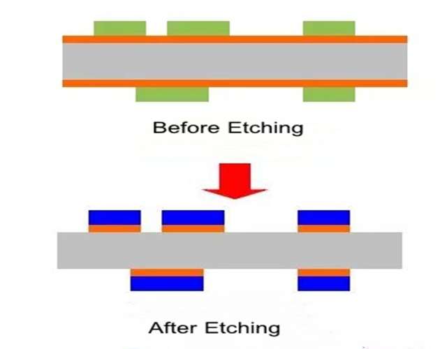
 E. Etching.
After the unexposed dry film or wet film is removed by the developer, the copper surface will be exposed, and then the exposed copper surface will be dissolved and corroded with acid copper chloride to obtain the required circuit.
E. Etching.
After the unexposed dry film or wet film is removed by the developer, the copper surface will be exposed, and then the exposed copper surface will be dissolved and corroded with acid copper chloride to obtain the required circuit.
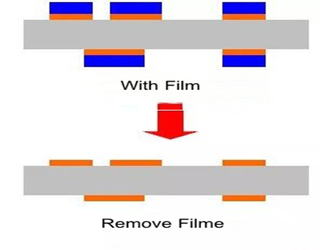
F. Remove the film.
Peel off the exposed dry film that protects the copper surface with sodium hydroxide solution to expose the circuit pattern.
 3. Browning.
Purpose: to form a microscopic rough organic metal layer on the inner copper surface to enhance the adhesion between the layers.
Process principle:
3. Browning.
Purpose: to form a microscopic rough organic metal layer on the inner copper surface to enhance the adhesion between the layers.
Process principle:
Through chemical treatment, a uniform organic metal layer structure with good adhesion characteristics is produced, and the surface of the copper layer before the inner layer is controlled to be roughened, which is used to enhance the adhesion strength between the inner copper layer and the prepreg after pressing.
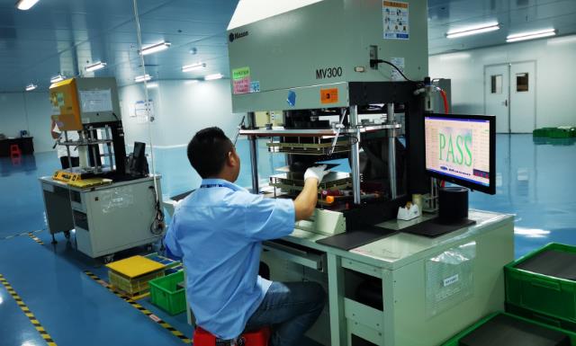
4. Lamination Pressing
Pressing is the process of bonding each layer of circuits into a whole by means of the adhesiveness of the pp sheet. This kind of adhesion is achieved by mutual diffusion and penetration between macromolecules on the interface, and then interweaving. The discrete multilayer board and pp sheet are pressed together to form a multilayer board with the required number of layers and thickness.
In actual operation, the copper foil, bonding sheet (prepreg), inner layer board, stainless steel, isolation board, kraft paper, outer layer steel plate and other materials are laminated according to the process requirements.
For designers, the first thing to consider when pressing is symmetry. Because the board will be affected by pressure and temperature during the lamination process, there will still be stress in the board after the lamination is completed. Therefore, if the two sides of the laminated board are not uniform, the stress on the two sides will be different, which will cause the board to bend to one side and affect the performance of the PCB.
In addition, even in the same plane, if the distribution of copper is not uniform, the resin flow speed at each point will be different, so that the thickness of the place with less copper will be slightly thinner, and the thickness of the place with more copper will be slightly thicker. Some.
In order to avoid these problems, various factors such as the uniformity of the copper distribution, the symmetry of the stack, the design and layout of the blind and buried holes, etc. must be considered in detail during the design.
5. Drilling
Through holes are generated between the circuit board layers to achieve the purpose of connecting the layers.
6. PHT
It is also called whole-board electroplating. The PCB board after drilling undergoes oxidation-reduction reaction in the sinking copper cylinder to form a copper layer so that the hole is covered with a layer of copper to achieve electrical communication between layers.
7. Panel Plating
Make the PCB board surface and the copper in the hole thickened to 5-8um on the PCB board that has just been copper-immersed to prevent the thin copper in the hole from being oxidized and micro-etched to expose the base material before pattern plating.
 8. Image Transfer
The process is the same as the inner layer.
8. Image Transfer
The process is the same as the inner layer.
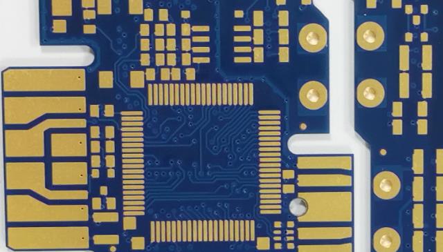
9. Pattern Plating & Etching
Increase the copper layer of the hole and circuit to a certain thickness (20-25um) to meet the copper thickness requirements of the final PCB board. And etch away the useless copper on the board surface, exposing useful circuit patterns.
10. Solder mask
Solder mask is one of the most critical processes in the production of printed circuit boards, mainly by screen printing or coating solder mask ink, coating a layer of solder mask on the board surface, and exposing through exposure and development. The disks and holes to be soldered are covered with solder mask on other places.
11. Silkscreen
The required text or part symbols are printed on the board surface by screen printing, and then exposed on the board surface.
12. Surface Finish
The solderability of bare copper itself is very good, but long-term exposure to the air is easy to be damp and oxidized, so the copper surface needs to be processed. The basic purpose of surface treatment is to ensure good solderability and electrical properties.
High Precision factory can supply the surface treatments,HAL lead or lead free, immersion gold, OSP, immersion tin,gold fingers, etc.
13. Routing
Cut the PCB into the required shape or size by CNC.
14. E-testing
Simulate the status of the board, and check the electrical performance if there is an open or short circuit.
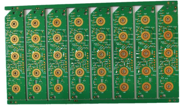
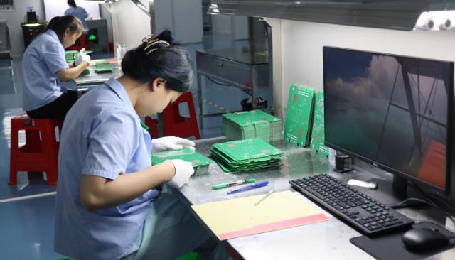
15. Final Inspection & Packing
Check whether the appearance, size, aperture, thickness, marking, etc. of the board meet customer requirements or not. And then pack the qualified board with vacuum packaging.
Need more details of Rigid PCB manufacturing,welcome to visit High Precision PCB factories in Dongguan or Hunan. info@gjzpcb.com