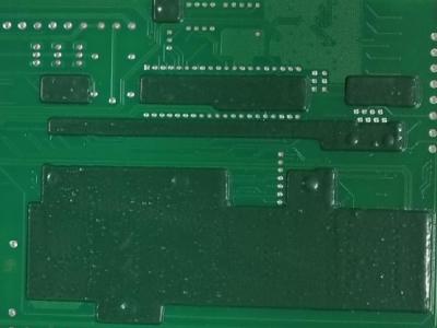
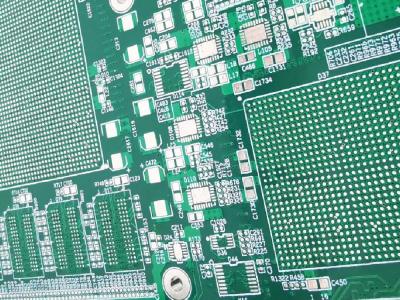
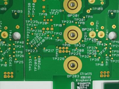
Specification:
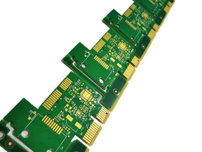
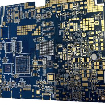
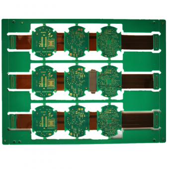
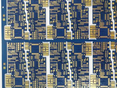
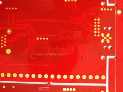
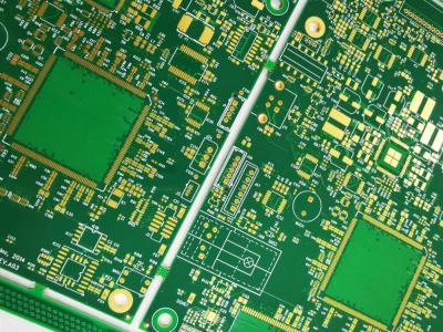
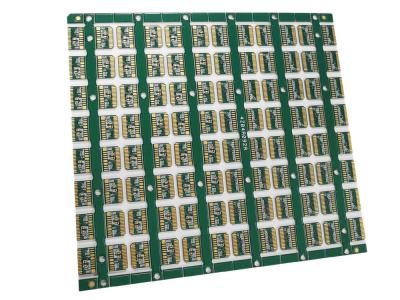
- Material: FR4 PCB
- Layer count: 6 layers
- Board thickness: 1.6mm
- Finish copper thickness: 1.0 oz
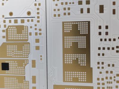
- Surface treatment: ENIG ( Immersion Gold )
- Application: Consumer electronics
|
Solder mask opening space between Gold finger and solder Pad (min.) |
8mil (0.2mm)
|
|
Plating Gold thickness of Gold finger (max.) |
Nickel:≥200u"(5.08um)
Gold:≥30u"(0.762um)
|
|
Plating Gold thickness of Gold finger (min.) |
NICKEL:≥100u''(2.54um)
GOLD:≥5u"(0.127um)
|
|
Space between gold finger and Tab (min.) |
3.4mm |
|
Bevel edge height of Gold finger (Angle:20°) (max.) |
T=1.6mm: 2.2mm
T=1.2mm: 1.65mm
T=1.0mm: 1.37mm
T=0.8mm: 1.1mm
|
|
Bevel edge height of Gold finger (Angle:30°) (max.) |
T=1.6mm: 1.39mm
T=1.2mm: 1.04mm
T=1.0mm: 0.87mm
T=0.8mm: 0.7mm
|
|
Bevel edge height of Gold finger (Angle:45°) (max.) |
T=1.6mm: 0.8mm
T=1.2mm: 0.6mm
T=1.0mm: 0.5mm
T=0.8mm: 0.4mm
|
|
Bevel edge height of Gold finger (Angle:60°) (max.) |
T=1.6mm: 0.46mm
T=1.2mm: 0.35mm
T=1.0mm: 0.29mm
T=0.8mm: 0.23mm
|
|
Tolerance of Bevel edge angle of Gold finger |
±5°, ±3° |
|
Tolerance of Bevel edge height of Gold finger |
<30°:7mil(0.178mm)
≥30°:5mil(0.127mm)
|
|
Thickness of peelable mask on Gold finger |
0.2-0.4mm |
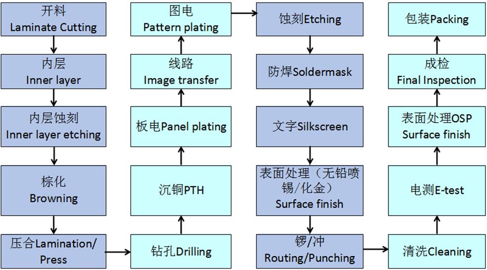
PCB Manufacturing Process Flow:
FAQ:
A. Why choose High Precision
Technology as PCB supplier?
-- High Precision Technology specialises on PCB manufacturing since 2011 with
rich experiences. We mainly use KB & Shengyi Brand laminiate, Rongda &
Taiyo brand oil and strictly compliance to IPC-6012 class 2. In our Hunan new
factory, all procedures are made in-house. The quality and price can be
controlled effectively. If you are still looking for a suitable supplier of PCB
fabrication, contact us, we will supply professional and flexible support.
B. What’s
kind of certificates do you have?
-- We have certificate ISO9001, ISO14001, UL, TS16949 etc.
C. What's
lead time?
-- The lead time can be negotiable
to meet your demands.
D. What is
MOQ (Minimum Order Quantity)?
-- There is no MOQ for new PN, sample is welcome.
E. What informations need to be supplied for quote?
-- Order quantity, Gerber file, PCB specification ( base
material, layer, PCB finished thickness, base copper thickness, surface
treatment, solder mask color, and others if you have )
F. Is the
files for quote or manufacturing safer?
-- Yes, it is safe as we are professional PCB manufacturer
and Non-disclosure agreement can be signed if you need. All documents from
customers are never shared with any third parties.
G. When can
the quotation be supplied?
-- All quotation can be supplied within 24 hours.
More enquiry,welcome to send us email.We will always give you professional service with 24H/7D online support.


